Researchers make progress in flexoelectric engineering of van der Waals ferroelectric CuInP2S6
Aug 29, 2022
Van der Waals layered CuInP2S6 (CIPS) has generated great excitement in recent years due to its room temperature ferroelectricity with out-of-plane spontaneous polarization, making it an ideal candidate to develop two-dimensional (2D) heterostructures for microelectronic devices.
Ferroelectric-field effect transistors, negative capacitance field-effect transistors, ferroelectric tunneling junctions, and memristors have all been demonstrated with CIPS, which are attractive for both logic and memory applications enabling future neuromorphic computing. However, field-driven polarization reversal of CIPS is intimately coupled with migration of Cu ions, often causing highly undesirable damage for device applications.

Assistant Professor Boyuan Huang’s group from the Department of Materials Science and Engineering at the Southern University of Science and Technology (SUSTech) has recently developed an alternative switching approach for CIPS utilizing the flexoelectric effect, abandoning the external electric field altogether.
This work, entitled “Flexoelectric engineering of van der Waals ferroelectric CuInP2S6,” was published in the journal Science Advances.
Their method is motivated by the strong correlation between polarization and topography variation of CIPS. Phase field simulation identifies a critical radius of curvature around 5 μm for strain gradient to be effective, which is realized by engineered topographic surfaces using silver nanowires and optic grating upon which CIPS is transferred. They also demonstrate the mechanical modulation of CIPS on demand via strain gradient underneath a scanning probe, making it possible to engineer multiple polarization states of CIPS for device applications.
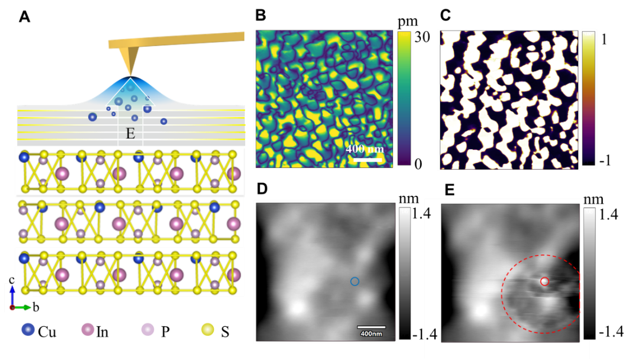
Figure 1. Structure and ferroelectricity of CIPS. (A) Schematic crystalline structure of CIPS and migration of Cu ion under a scanning probe. (B, C) typical vertical PFM amplitude (B) and phase (C) mappings. (D, E) AFM topography mappings before and after ±6 V applied via scanning probe tip, exhibiting field-induced damage as revealed by topography change.
In principle, it is possible to apply a larger DC voltage to switch the spontaneous polarization of CIPS, as schematically shown in Fig. 1A. But when a DC voltage of ±6 V is applied through the scanning probe, substantial topographic change is observed in Fig. 1(D and E) due to ionic migration induced damage. In other words, the strong coupling between polarization and ionic migration makes it quite challenging to manipulate CIPS polarization electrically.

Figure 2. Domain evolution associated with topography variation as revealed by vertical PFM amplitude and phase mappings, both imposed on 3D AFM topography. (A) Protrusions. (B) Wrinkles. (C) A bubble. (D) Schematic flexoelectric effect. Image size: (A), 2 μm; (B, C), 5 μm.
Prof. Huang’s team observed the strong correlation between polarization and topography of CIPS, as shown in Fig. 2, suggesting that strain gradient may be important. When there is an upward bending in CIPS, the upper part of the flake is elongated. In contrast, the lower part is shortened, and this strain gradient propels Cu ions into a position of upward polarization where the free volume is larger. When it is bent downward, the opposite occurs, known as the flexoelectric effect.
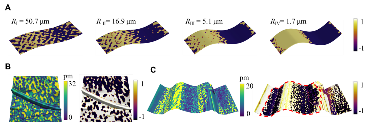
The result raises an interesting prospect of flexoelectric engineering of CIPS, and to this end, the researchers carried out a phase field simulation first to verify its feasibility. When the radius of curvature of the substrate is reduced from 50.7 μm to 5.1 μm, the domains in Fig. 3A are seen to gradually combine with each other, with upward polarized domains growing in the peak regions and downward polarized domains growing in the valleys. To further realize this in an experiment, they designed a process of transferring a CIPS flake onto a substrate with a silver nanowire of 20 nm diameter. The part covering the silver nanowire becomes uniformly polarized, as seen in Fig. 3B. They also transferred CIPS onto an optic grating with a period of 3 μm, as shown in Fig. 3C, and again observed upward polarization in the peak region and downward polarization in the valley.
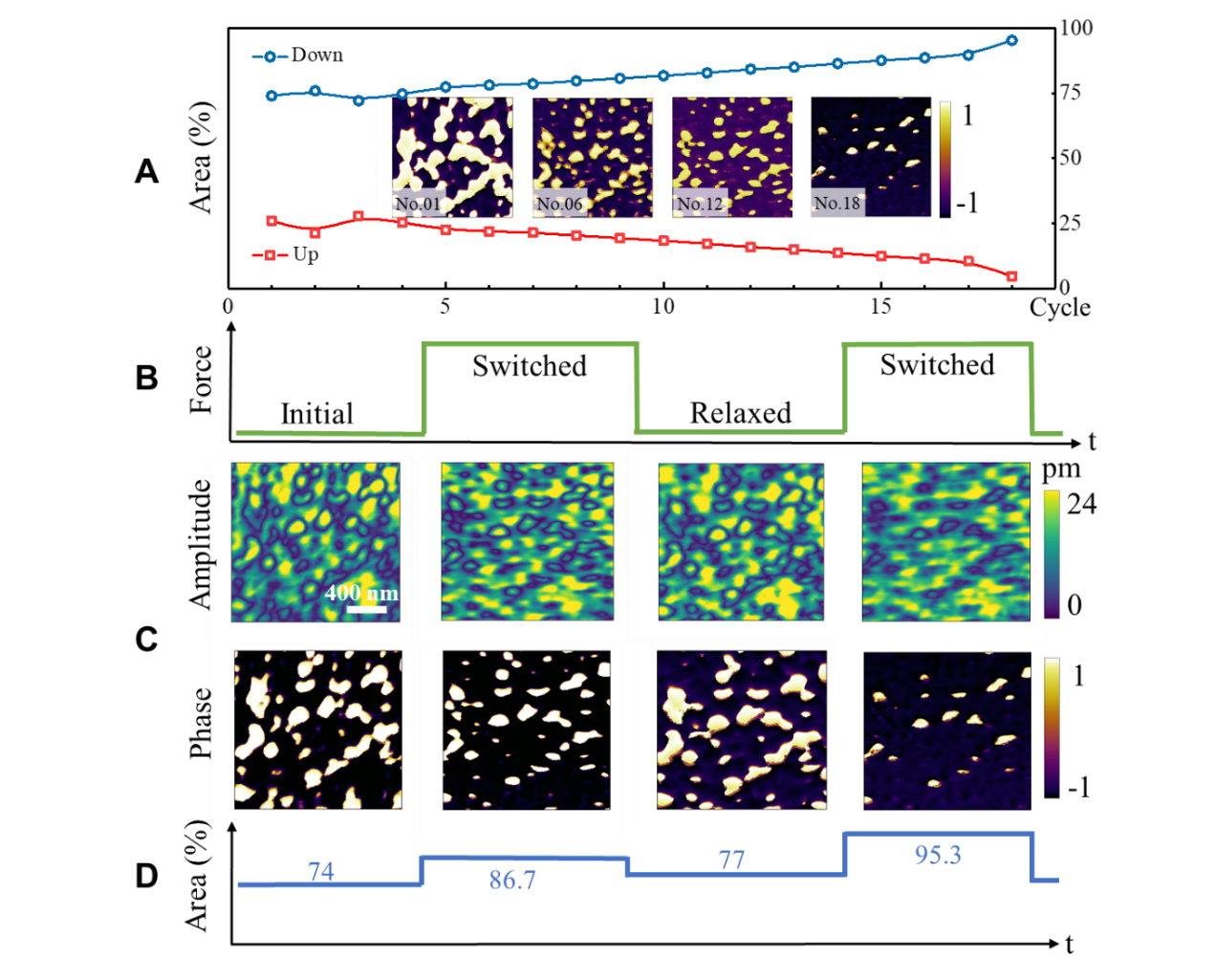
Figure 4. Mechanical modulation of CIPS. (A) Variation of polarization with cycles of mechanical scans. (B) Schematics of initial, switching, relaxation, and another switching stage with two states of tip forces. (C) The corresponding vertical PFM amplitude and phase mappings in the four stages. (D) Percentage of downward polarization in the four stages.
Finally, the researchers demonstrated mechanical modulation of CIPS on demand via scanning probe-induced flexoelectric effect, as shown in Fig. 4. Here, the polarization of CIPS can be mechanically modulated to multiple states by cyclic mechanical scans, a process mimicking synaptic plasticity. The polarization switch also enjoys a long relaxation time, and such non-volatility is ideal for long-term potentiation in neuromorphic computing.
Visiting Ph.D. student Wenjie Ming of Xiangtan University, Asst. Prof. Boyuan Huang of SUSTech, and Ph.D. student Sizheng Zheng of Zhejiang University are the co-first authors of this paper. Asst. Prof. Boyuan Huang, Prof. Jie Wang of Zhejiang University, and Prof. Jiangyu Li of SUSTech are the co-corresponding authors. Other collaborators include Ph.D. student Yinxin Bai and Prof. Junling Wang of SUSTech, and SUSTech is the first corresponding unit.
The work was supported by the National Natural Science Foundation of China (NSFC), Leading Talents Program of Guangdong Province, Guangdong Provincial Key Laboratory Program, Guangdong Basic and Applied Basic Research Foundation, Key Research Project of Zhejiang Laboratory, Shenzhen Science and Technology Program, and the Guangdong Provincial Department of Education Innovation Team Program.
Paper link:
Latest News

Related News


 8F, South Tower, College of Engineering, 1088 Xueyuan Avenue, Shenzhen 518055, P.R. China

 coe_public@sustech.edu.cn
 WeChat