Researchers make progress in new method for investigating interlayer shear thermal deformation in atomically-thin van der Waals layered materials
Aug 03, 2022
Possessing outstanding mechanical properties (i.e., high in-plane stiffness and bending flexibility), atomically-thin vdW materials offer a unique platform for strain engineering. Mechanical and thermal approaches are the most commonly adopted methods to introduce strain in vdW materials.
For example, the lattice can be deformed by using a patterned substrate, generating nanobubbles in vdW materials and bending flexible substrate, based on which intriguing physical phenomena and applications have been discovered. However, investigations on resolving the thermal deformation layer by layer in vdW materials are scarce due to the lack of an effective characterization strategy.

Assistant Professor Xiaolong Chen’s research group from the Department of Electronic and Electrical Engineering at the Southern University of Science and Technology (SUSTech) has recently published their research results, where they reported a new optical approach for in-plane shear thermal deformation (STD) and interlayer shear thermal deformation (ISTD) in atomically-thin van der Waals (vdW) layered materials.
Their study, entitled “Probing interlayer shear thermal deformation in atomically-thin van der Waals layered materials,” was published in Nature Communications, a multidisciplinary journal covering the natural sciences, including physics, chemistry, earth sciences, medicine, and biology.
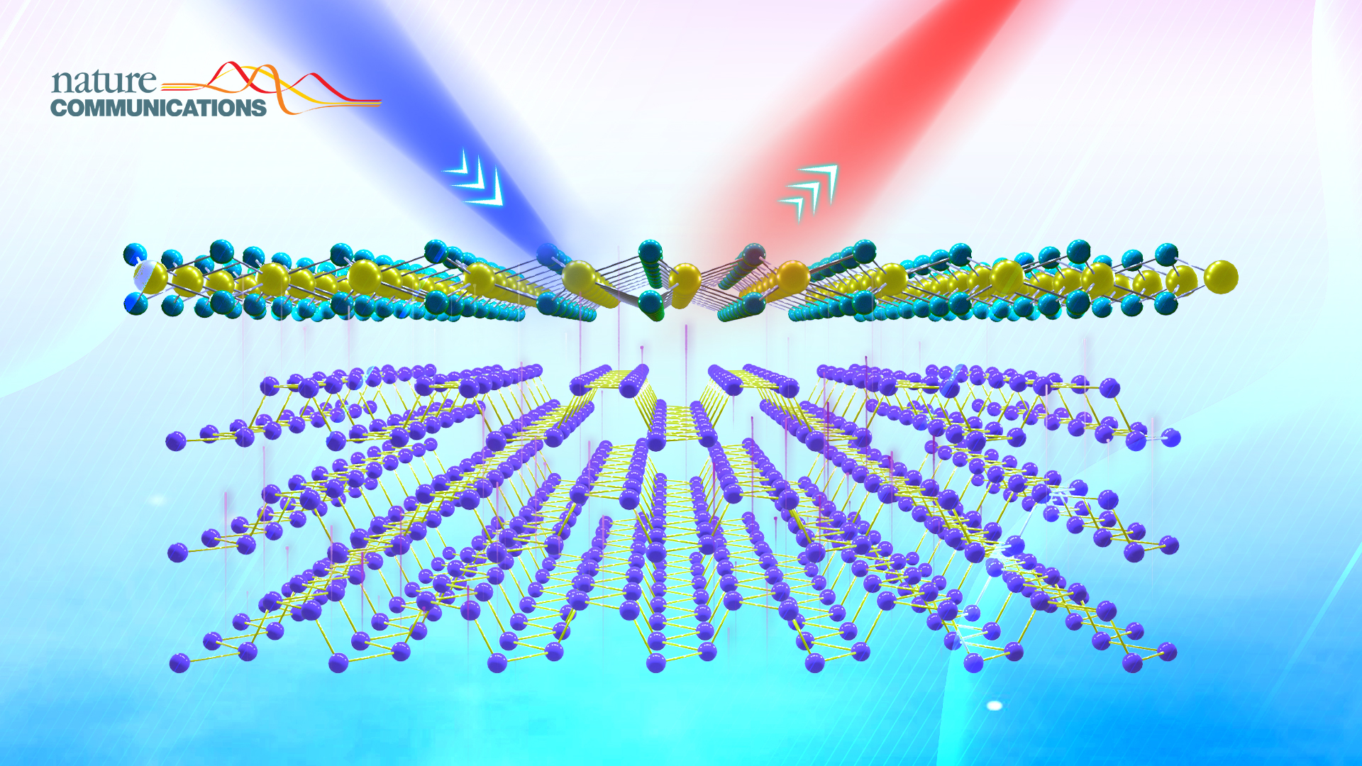
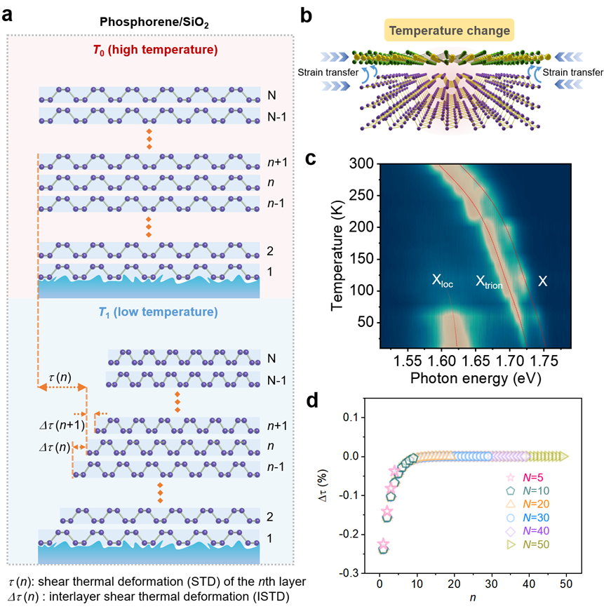
Monolayer WSe2 is a direct-bandgap semiconductor with very high luminescence efficiency. Its strain-sensitive optical and electronic properties have been widely investigated. In view of this, Prof. Chen’s team designed a WSe2-based vertical vdW heterostructure. The top monolayer WSe2 serves as an in-situ “strain meter”, which can directly probe the mechanical behaviors of the underlying vdW materials (i.e., phosphorene) through monitoring the temperature-dependent photoluminescence spectra (see Figure 1).
An effective ISTD model was established, considering interlayer interactions at both homo- (phosphorene-phosphorene) and hetero-interfaces (phosphorene-WSe2), and Young’s modulus and TEC of phosphorene and WSe2. By combining experimental results and theoretical modeling, the STD and ISTD of each individual layer in phosphorene can be resolved quantitatively. Moreover, the approach also allows access to the temperature-dependent thermal expansion coefficient of phosphorene, and the interlayer coupling coefficients at the homo- and hetero-interfaces.
This work exploits the strain-dependent optical properties to probe the in-plane STD of vdW materials. It establishes an effective ISTD model, providing useful information for strain engineering in vdW materials.

Figure 1. a) ISTD model of an N-layer phosphorene/SiO2 system when temperature decreases from T0 to T1. b) Schematic image for the WSe2/phosphorene heterostructure for ISTD investigations. c) Temperature-dependent photoluminescence spectra of WSe2. d) The ISTD in phosphorene obtained from the experimental and theoretical results.
Ph.D. student Le Zhang and master’s student Han Wang are the co-first authors of this paper. Asst. Prof. Chen Xiaolong of SUSTech and Prof. Wang Lin of Nanjing Tech University are the co-corresponding authors, while SUSTech is the first corresponding unit.
The work was supported by the National Natural Science Foundation of China (NSFC) and the National Key R&D Program of China.
Paper link:
Latest News
Related News


